
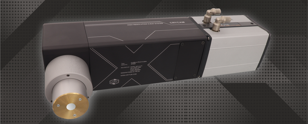
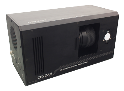
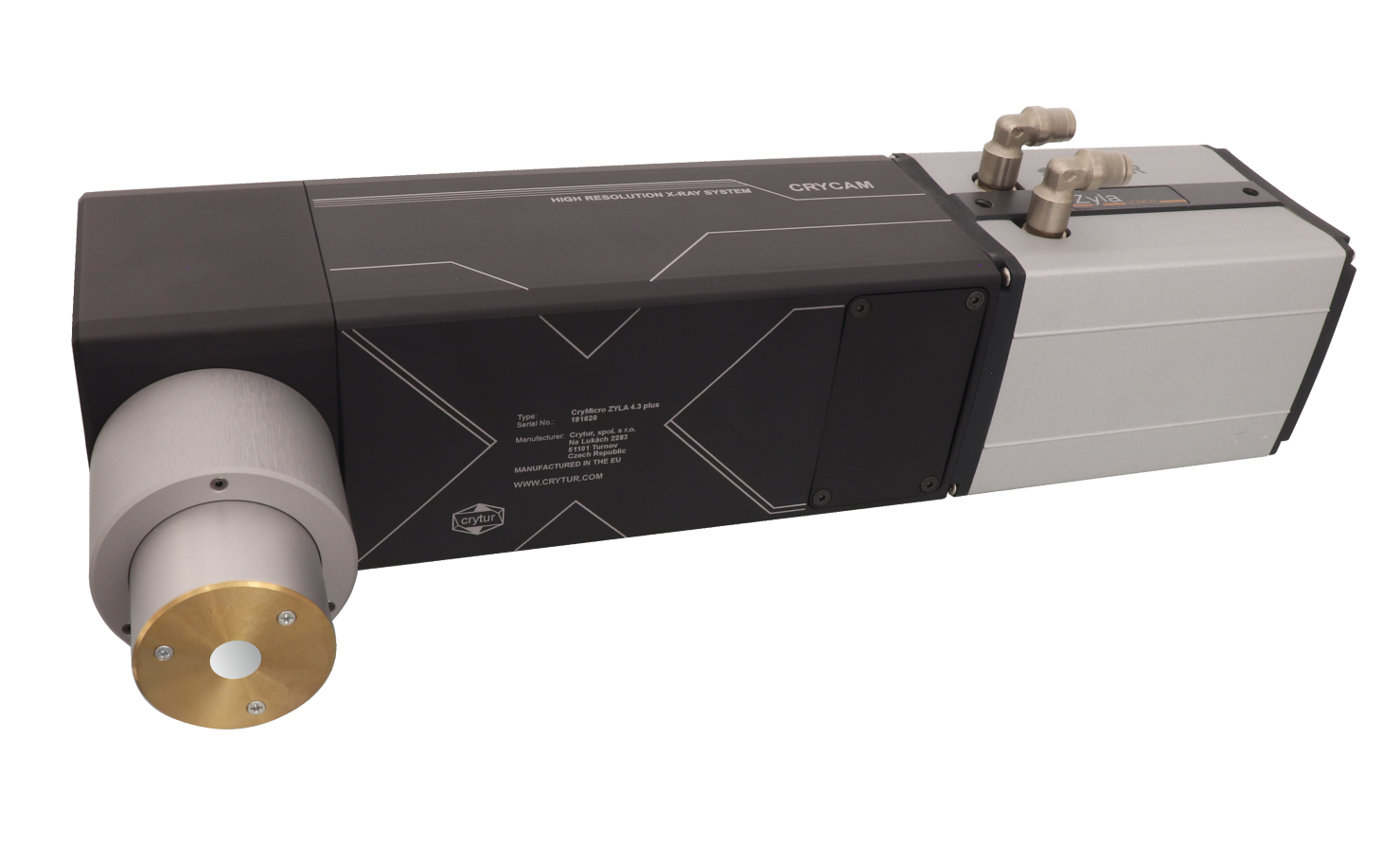
Crycam™ X-ray camera
Key characteristics
|
 |
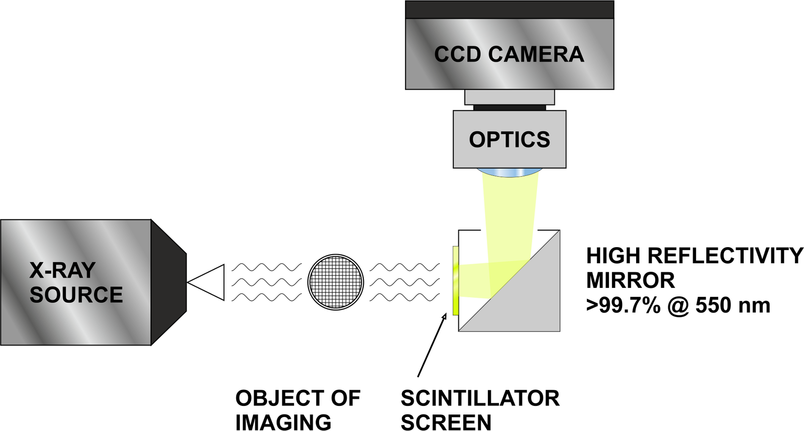
Imaging system scheme
Ultra-thin single crystal screens
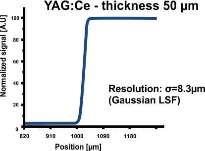
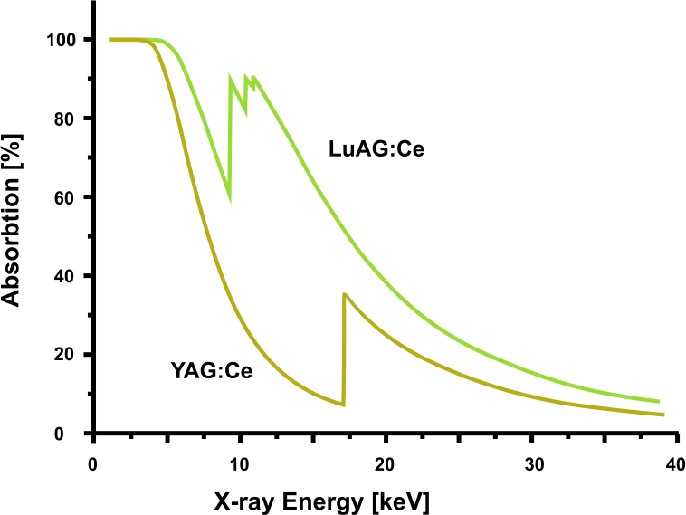 YAG:Ce and LuAG:Ce imaging screens are quite suitable for electron beams, proton beams, low energy X-ray, UV light, VUV and XUV radiation. Submicron spatial resolution is achieved due to excellent properties of the material and precise manufacturing.
Single crystal screen properties:
- High optical quality
- High homogeneity of luminescence
- Extreme thinness and excellent face parallelism
- Chemical and temperature resistance
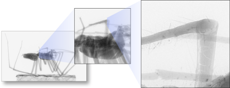
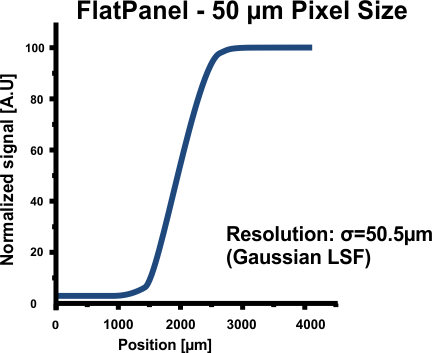
Crycam™ delivers considerably better resolution than an ordinary flat panel.
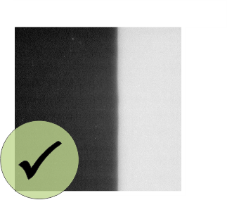
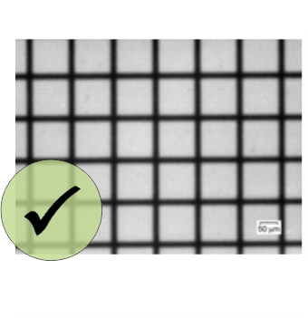
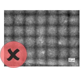
| Image comparison of 100 µm iron plate edge | Image comparison - golden mesh | Image comparison - head of wasp | |
|---|---|---|---|
 |
 |
 |
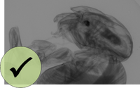 |
| YAG:Ce Crycam™ | YAG:Ce Crycam™ | YAG:Ce Crycam™ | YAG:Ce Crycam™ |
 |
 |
 |
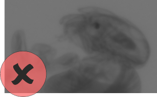 |
| Flat panel P43 scintillator | Flat panel P43 scintillator | Flat panel P43 scintillator | Fibre optics plate with CsI:Tl scintillator |
MACRO SYSTEM |
MICRO SYSTEM |
|
|
 |
 |
Technical parameters
Main features
- 16-bit monochrome depth
- Low electronic read noise - several e-/pix/s only (slow reading)
- Peltier cooling
- Suitable for low light sources
- Can be used for light intensity measurements
Parameters
Shutter: Yes
Binning: 1x1 to 4x4.
Reading: Two modes, standard and low-noise.
Frames accumulation: Yes.
CCD signal processing: correlated double sampling (CDS) + 16 bit A/D converter.
Image acquisition: Fully SW controlled
Features: Background subtracting, Flat-field correction.
Antiblooming: SW controlled, Interline Transfer CCDs only.
Cooling: Peltier driven, <50°C below the ambient temperature
Optionally: FAN / cooling water.
Data interface: USB 2.0.
Power source: 12 VDC/ 5 A/ 100-240 V/ 50-60Hz
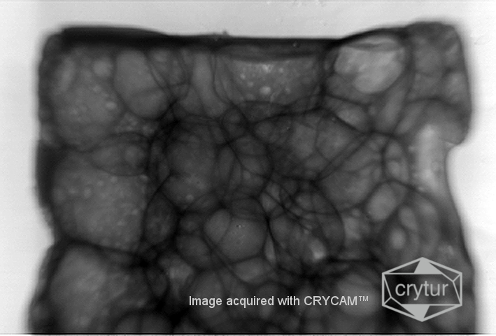
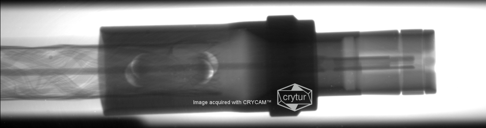
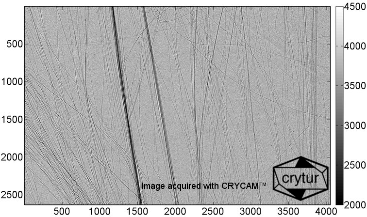
Sample images
Biological and medical objects
Electronics - integrated circuit inspections
Light-weight materials with pores
X-ray, UV, synchrotron beam inspection and measurements
Highly detailed X-ray ND inspections
Composite material inspection and development
The imaging system can be used in many applications where very small details of imaged object should be observed
 |
 |
 |
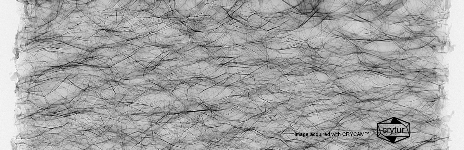
| Alumina foam | A connector with shielded cable | Carbon fibres (7-10 micron) |
 |
 |
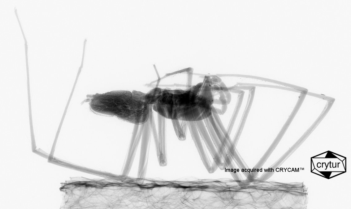 |
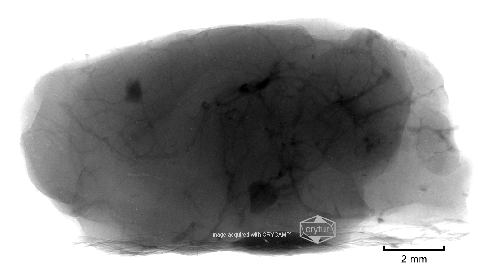
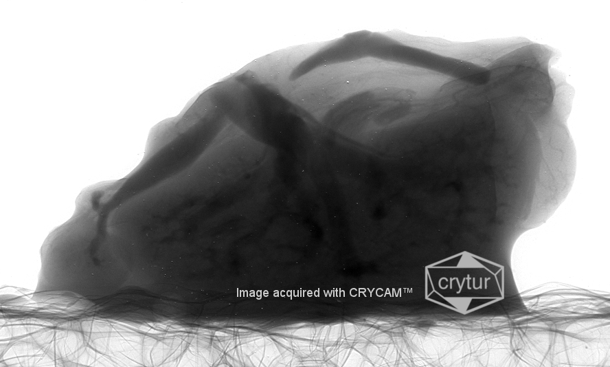
| Mouse brain | Mouse kidney | Spider |
 |
 |
 |
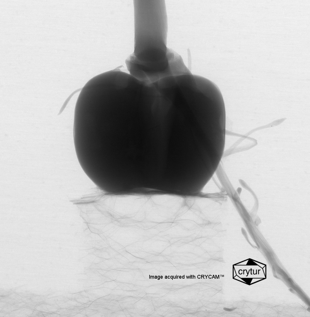
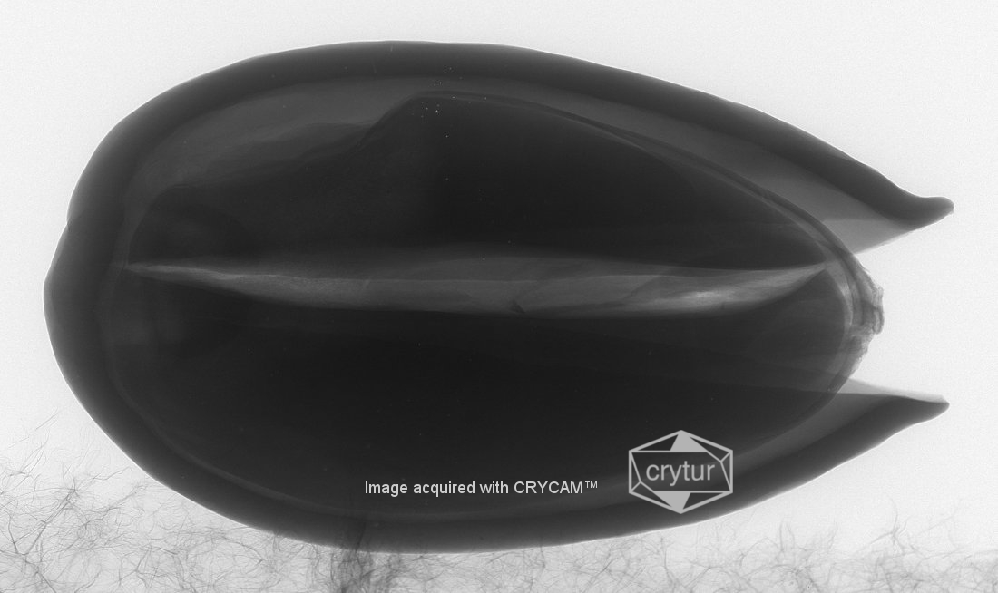
| Pea (sprouting) | Pistachio seed | Plastic foam |


